Analog Devices: Helping Achieve Net Zero CO2 Emissions with Single-Pair Ethernet

Written by Meghan Kaiserman, Strategic Marketing Director

Abstract

To meet net zero CO2 emission goals, the building sector needs to modernize its communication infrastructure. This article shows how single-pair Ethernet, specifically 10BASE-T1L, enables the easy retrofitting of buildings using legacy links like RS-485 to improve digitization, enable automation, improve security, and substantially lower energy consumption to achieve greater sustainability.

Introduction

To address climate change and sustainability, over 90 countries are actively developing net zero CO2 emission policies. In short, net zero is achieved when human-based CO2 emissions are both reduced and counterbalanced through other activities.

A fundamental factor in reaching net zero is the reduction of CO2 emissions across all industries. However, according to the International Energy Association (IEA), the building sector is not on track to meet global 2050 net zero CO2 emission goals. Specifically, 2030 goals target 35% less energy consumption per square meter compared to 2021.1 As buildings account for 30% of global energy consumption today, there is concern that emission goals will not be met unless the industry takes specific action to digitize systems and implement automation. Further complicating the challenge is that to implement effective automation, more real-time data capture is needed at a level that exceeds the current throughput capacity and responsiveness of legacy RS-485-based infrastructure. In addition, connecting devices and building systems to the network exposes them to cyberattacks, requiring advanced security beyond the current capabilities of these legacy networks.

This article explores how single-pair Ethernet can help the building industry meet net zero goals while supporting AI-based automation in a secure and cost-effective manner. Single-pair Ethernet enables long-reach connectivity to the edge for both greenfield and retrofit installations, making it a critical tool for seamless data transfer between IT and OT domains.

Energy Savings Through Digitalization

The IEA 2030 Net Zero plan3 requires a ~15% reduction in emissions by reducing demand through techniques like behavioral changes and digitalization. While teaching people how to conserve energy can be effective, IEA case studies4 point to automation rather than behavior change as having the most potential for energy reduction.

Increasing digitalization of commercial buildings will enable operators to not only measure operational improvements but also provide the foundation for operational automation. With access to the right sensor data and control capabilities, it is possible to optimize the operation of buildings to reduce energy consumption while best serving the people within.

For example, the need to improve indoor air quality places additional demands on building operations. New regulations such as ANSI/ASHRAE 62.1 require the intake of more outdoor air, and additional amounts2 may be required to ensure best practices for health and hygiene. These ventilation standards will result in increased energy consumption, meaning energy demand will need to be further reduced. To achieve optimal operation, the many HVAC systems within a building need to be able to work together to avoid having the systems work at cross purposes.

Converging operations of disparate HVAC, lighting, fire, and access control systems requires access to the right data and controls. These allow AI and machine learning (ML) optimization to determine the ideal use of light, heating, or cooling based on people’s current and planned activity. They also allow control of airflow to help ensure proper indoor air quality while balancing energy consumption.

However, it is hard to converge data from multiple systems with separate vendors maintaining separate databases, leading to data siloes. According to the IEA group working on data sharing guidelines5 for buildings and HVAC systems, the challenge then is to bring diverse data sources together in a single pane of glass, so that trends can be compared, and analytics applied, to yield new insights, as shown in Figure 1.

Modernizing the Communications Infrastructure

Key to merging the many different data sources within a building is the measurement and connectivity infrastructure being used. Traditionally, sensors and controls in commercial buildings have been connected through wired serial communication links using RS-485 transceivers and protocols like BACnet™, Modbus, and LonWorks.6

RS-485, however, is a legacy interface that is limited in both throughput and security. For example, the maximum baud rate for BACnet MS/TP, a common building automation protocol, running on an RS-485 physical layer is 115.2 kbps.10 In addition, legacy communication protocols like BACnet and Modbus were designed for closed networks and lacked built-in encryption and authentication capabilities. This creates a large cybersecurity threat as these devices are connected to the internet through gateways to IT infrastructure.

Single-pair Ethernet, specifically 10BASE-T1L, is an exciting new communication method ratified on November 2019, IEEE 802.3cg, which is now being deployed in buildings.9 Wired serial link cable used for RS-485 runs can be reused with 10BASE-T1L Ethernet data running over it. Thus, existing infrastructure can be adapted to single-pair Ethernet. This has many benefits:

  • Nodes can now support higher bandwidths of up to 10 Mbps.
  • Nodes are IP addressable, simplifying the management of devices.
  • Reach increases to 1 km, which is enough to support the maximum lengths used for existing RS-485 cabling runs. This is a marked improvement over standard 10 Mbps/100 Mbps Ethernet’s limit of just 100 m.11
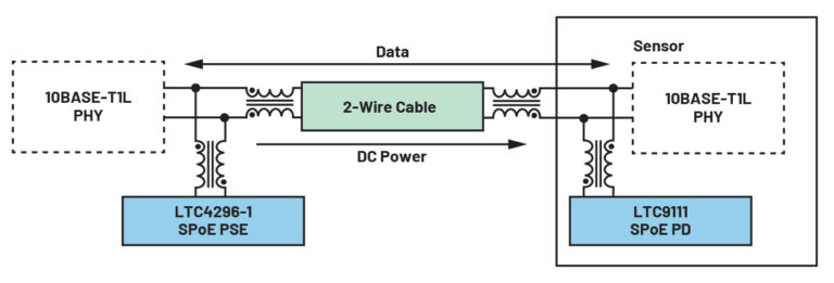
  • IEEE 802.3cg specifies Class 15 and allows up to 52 W of power to be sent over single twisted pair cable along with 10BASE-T1L data. With the recently released LTC4296-1 power over Ethernet (PoE) controller, systems can deliver power to a wide range of end devices. Note that due to variations in cable quality, power delivery is recommended for new installs only.

As a first step in the digitalization journey, building controllers using standard 10 Mbps/100 Mbps Ethernet have been deployed, communicating with Ethernet-based versions of these legacy protocols, called BACnet/IP and Modbus TCP/IP.6 BACnet/IP devices use the same data objects as BACnet MS/TP legacy devices, so it is easy to implement a system with both types of devices. Ethernet-connected installs with IP-based protocols like BACnet/IP and Modbus TCP/IP that support modern cybersecurity measures are on the rise.12 BACnet has about 60% market share7 worldwide and about 80% of new installs are using wired RS-485-based serial communications. The Building Services Research and Information Association (BSRIA) estimated that in 2019, 5% of HVAC sensors were wireless with lower connection reliability and the need for batteries limiting where this can be adopted.8

Improved Communications

Heating and cooling systems have multiple components that need to exchange information to achieve the temperature set point, including thermostats, controllers, air handling units, and variable air volume units. Speeding up the frequency of communication from common serial baud rates of 9.6 kbps to 115.2 kbps to an Ethernet bandwidth of 10 Mbps means the data throughput of the system has increased substantially. There are several important benefits that come with such high speed IP-based communications.

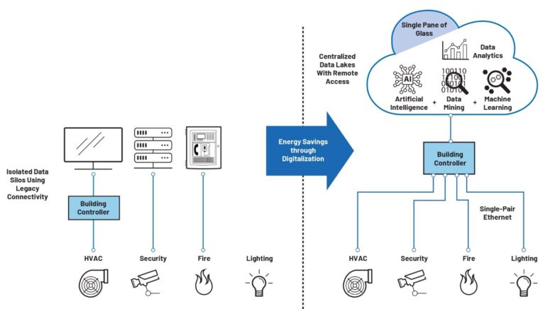
Figure 1. Converging systems allow data visualization through a single pane of glass, which enables energy savings when used alongside automation and AI/ML.

Analytics, not samples: The slow data rates of legacy communication meant building managers had to prioritize what data they collected and sample the data they did collect. With single-pair Ethernet, managers can stop worrying about serial communication sampling rates and focus on developing the wide range of advanced analytics they can now perform with the additional data that can be collected from the system.14

Energy savings: Additional data enables greater energy savings through faster control loops or computationally intensive energy optimizations using models and real-time sensor inputs.

Converged data/elimination of data siloes: Legacy-wired serial communications require a gateway to convert data from edge devices into Ethernet-based packets before passing them to the cloud. Upgrading wired serial communication links to single-pair Ethernet, 10BASE-T1L, allows these gateways to be eliminated while reusing the existing cabling. This avoids data siloes, reduces failure points, eliminates the cost of gateways, and drives down overall latency.

Real-time responsiveness: Communication protocols and software running on gateways slow down response time to the order of seconds, while building automation applications such as IO monitoring may require 100 millisecond or lower latency.13 The higher throughput of single-pair Ethernet combined with the elimination of gateways means faster throughput so systems can respond in real-time.

Secure Communication

Memoori12, a leader in smart buildings research, cites that the lack of effective cyber cover is rapidly becoming the leading barrier to smart building adoption moving forward.

One of the biggest challenges faced with building digitalization is converging the IT and OT domains. It is possible to retrofit security into legacy RS-485-based field bus OT networks by upgrading to protocols like BACnet/SC, but this is costly, time-consuming, and can easily miss vulnerabilities in the existing system. Effective security is critical as building automation systems received the most cyberattacks among all industrial control systems, higher than oil and gas, energy, and automotive manufacturing in a 2020 study by Kaspersky.15

To secure communications, the legacy wired serial communication protocol BACnet has been adapted to BACnet/SC12, which supports secure communications on a wired serial link allowing encryption. However, all BACnet devices on the network need to be upgraded simultaneously to take full advantage of these new capabilities. Existing equipment using legacy BACnet will need to be redesigned and serviced to add the additional cryptography functions required for BACnet/SC. Single-pair Ethernet, specifically 10BASE-T1L, allows an edge node that had been connected using wired, insecure serial communications like BACnet to be upgraded and connected using BACnet/IP protocol running Ethernet-based security. Importantly, this new and improved security posture is achieved without running new, costly Ethernet cables along existing signal paths.

By upgrading devices on OT networks to run secure Ethernet-based protocols, much of the risk associated with cyberattacks can be mitigated. Single-pair Ethernet, 10BASE-T1L, has the promise of enabling the transition from insecure legacy communication to secure Ethernet-based communications with one generation of hardware upgrades while reusing existing wiring infrastructure.

Single-pair Ethernet, 10BASE-T1L, is an important technology that brings IP connectivity to the edge, improving security, reusing wiring, converging IT and OT networks, and even delivering power. With significantly higher throughput, elimination of gateways, and advanced security, single-pair Ethernet will help the building industry achieve the IEA Net Zero 2030 goal of reducing emissions by 15%. Modernizing the communication infrastructure of buildings will provide access to a tremendous amount of real-time data within a building while eliminating data siloes and enabling a single pane of glass approach to management. In addition to allowing faster control loop closure for conventional control schemes and supporting artificial intelligence and ML optimizations, managers will be able to generate actionable insights that result in substantial energy savings.

Analog Devices has a team focused on the sustainable buildings market and is a leader in technologies enabling digital transformation such as single-pair Ethernet (10BASE-T1L), security and intelligent IOs, as well as isolation and wired RS-485 transceivers for legacy systems. Analog Devices has several released single-pair Ethernet products enabling point-to-point (ADIN1100, ADIN1110) as well as line-and-ring architectures (ADIN2111).16 For single-pair power over Ethernet, please see the LTC4296-1 on the power sourcing side and LTC9111 on the device side.


References

1Buildings.” International Energy Association.

2New Ventilation Design Criteria for Energy Sustainability and Indoor Air Quality in a Post COVID-19 Scenario.” Renewable and Sustainable Energy Reviews, Vol. 182, 2023.

3 Net Zero by 2050—A Roadmap for the Global Energy Sector. International Energy Association, 2021.

4 Energy Efficiency 2021. International Energy Association, 2021.

5 IEA Annex 81 Activity A1—A Data Sharing Guideline for Buildings and HVAC Systems. International Energy Association, 2023.

6 The Ultimate Guide to Building Automation Protocols. Smart Buildings Academy, 2020.

7Research Study Indicates BACnet Global Market Share over 60%.” BACnet International, 2018.

8A New Detailed US Field Device Study Is Released.” BSRIA, 2020.

9Single Pair Ethernet on Its Way into the Smart Building.” Smart Buildings Technology, 2020.

10 Improving BACnet®. BACnet, 2020.

11How to Cost-Effectively Network Sensors for Building Management Systems.” DigiKey, 2023.

12Cyber Security in Smart Commercial Buildings 2022 to 2027.” Memoori, 2022.

13Industry 4.0 for Energy Productivity.” RACE for 2030, 2021.

14How IP Controls Are Changing Building Automation Controls.” ControlTrends, February 2022.

15Threat Landscape for Industrial Automation Systems.” Kaspersky, March 2021.

16Building Automation Controllers and Networks.” Analog Devices, Inc.

About the Author

Meghan Kaiserman is the strategic marketing director for sustainable buildings at Analog Devices and is focused on digitalization technologies including intelligent IO, single-pair Ethernet, and security. Meghan has over 18 years of service at Analog Devices and previously held roles in applications and systems engineering. She has developed products for the industrial market ranging from precision analog to energy measurement and Industrial Ethernet. Meghan received a B.S.E.E. from the Cooper Union for the Advancement of Science and Art in New York City.


Disclaimer: This article has been published with explicit permission from Analog Devices Inc. (ADI), who has granted Excelpoint the rights to produce and share this content on our platform. All information, insights, and viewpoints are provided in collaboration with ADI, ensuring authenticity and accuracy. No part of this article may be reproduced or utilized in any form or by any means without prior written consent from ADI and Excelpoint.

Eggtronic: The Future of Flyback

Topologies to Improve Low-Power AC/DC Flyback Conversion

From TVs, computers to gaming consoles and printers, the electronic products in our homes and offices all demand efficient conversion of AC from the wall outlet to the DC used by the active components within the device. And with the exception of kitchen appliances and products such as electric heaters and hair dryers, the majority of these devices are likely to be classified as ‘low-power’, operating at 100 W or below.

Most of the devices in our home or office require low-power AC/DC conversion

In some cases, the AC/DC converter is embedded in the product itself, while others – – including smart home assistants and computer peripherals – have a dedicated external power supply. AC/DC conversion is also fundamental to the adapters used to charge mobile phones, tablets and other portable devices.

While the low power nature of these applications might imply that efficiency is not a huge concern this is not the case. Given the billions of these devices that are in use and that are often left plugged in 24 / 7 the impact on global energy consumption and subsequent emissions is significant. Making AC/DC converters more efficient is, therefore, at the top of the power engineer’s design agenda.

Traditional Approach to Low-Power AC/DC Conversion

Thanks to its versatility, performance and simplicity, the so-called ‘flyback’ topology – which generally comprises a primary-side MOSFET, output (secondary) rectifier diode, output capacitor and flyback transformer and a few other minor components – has been a popular choice for low-power AC/DC conversion for many years.

Figure 1. Simple flyback converter

A version of the topology known as quasi-resonant (QR) flyback has become particularly popular as it enhances efficiency and performance by reducing switching losses through the lowering of primary MOSFET drain-source voltage before the turn-on pulse. This voltage lowering is achieved using a resonance between the transformer inductance and the parasitic capacitance of the power MOSFET, which reduces the energy dissipated as the parasitic MOSFET capacitance is discharged before the MOSFET is turned on.

Figure 2. Quasi-resonant (QR) flyback converter

Waveforms of the MOSFET voltage and corresponding primary and secondary currents are shown below.

After the energy stored in the transformer is fully discharged to the secondary, oscillation occurs across the MOSFET drain. This is caused by the primary inductance and the capacitance seen across the MOSFET drain-to-source. The voltage ringing, which depends on the reflected voltage VR, will produce minimum valley points. When the controller detects the minimum valley point, it turns on the MOSFET for QR or valley switching flyback operation.

QR efficiency gains are primarily realized in full-load with 110V AC grid input, when this architecture is at almost Zero Voltage Switching. At light loads, and when the input is 240 V (i.e. EU grid), efficiency is generally lower because hard switching cannot be avoided.

The QR flyback design can be further improved by implementing zero-voltage switching (ZVS). As stated, in a normal QR flyback design the MOSFET is switched in a ‘valley’ where the drain-source voltage (VDS) is at a minimum, but not necessarily zero. With ZVS (or soft switching), VDS falls to zero before the MOSFET is switched. This not only minimizes losses but reduces electromagnetic interference (EMI).

A more recent evolution is active clamp flyback (ACF) architecture, which uses the energy stored in the transformer’s leakage inductance that would have been dissipated in a passive clamp snubber resistor. Delivering this ‘recycled’ energy to the load improves converter efficiency and significantly reduces the peak voltage across the MOSFET during turn-off. What’s more, the QR ‘valleys’ in an ACF design are significantly lower, often achieving near-ZVS operation, supporting reduced switching losses and lower EMI.

Figure 3. Active clamp flyback (ACF) converter

Flyback Evolution

Designers looking to further enhance performance, efficiency and reliability of AC/DC converter designs now have a further option. Known as QuarEgg®, this innovative evolution of the flyback topology significantly improves the efficiency and reduces the size of AC/DC converters that would normally have been based upon ACF and QR flyback topologies. Unlike other approaches, QuarEgg operates with ZVS under all load conditions to give very flat efficiency curves, delivering up to 95% at full load and up to 92% at light load. What’s more, in standby mode, a QuarEgg-based design consumes less than 18 mW.

Figure 4. Comparison of QuarEgg and QR flyback efficiencies

Compared to a generic QR flyback topology, the new approach adds a low-voltage, low-cost MOSFET on the secondary side in parallel to the SR MOSFETs, which is used mainly for the Zero Voltage Switching (ZVS). The main QuarEgg controller is on the secondary side of the converter so as to enhance output voltage regulation, which integrates the synchronous rectification control as well as the power delivery (PD) control. The elimination of a high-voltage, high-side clamping MOSFET reduces overall component count and improves reliability.

Figure 5. Simplified schematic of QuarEgg AC/DC converter

The ZVS MOSFET is essentially included as a means of actively forcing ZVS for the primary power MOSFET across all load conditions. While the converter is switching, the secondary side controller senses the VDS of the primary MOSFET via the secondary winding. When each crest occurs, the ZVS MOSFET turns on, allowing a small amount of current to be injected in the power transformer, after which it turns off and that energy is rectified and recovered at primary side, discharging the drain node so VDS becomes zero, thereby ensuring a ZVS turn-on of the primary MOSFET.

Figure 5. Key KPIs for QR, ACF and QuarEgg AC/DC conversion solutions

The new topology can be used with all types of MOSFET switching devices, including legacy silicon and wide bandgap (WBG) materials such as gallium nitride (GaN) and silicon carbide (SiC). With improved performance compared to conventional ACF and QR topologies, QuarEgg-based power converters are up to seven times more efficient and three times smaller than traditional silicon converters and up to three times more efficient and twice as small as already high-performance GaN converters.

For more information about topology QuarEgg and controller EPIC1AFQ01, we invite you to visit Eggtronic official website at the following links:

https://www.eggtronic.com/power-converters/quaregg/

https://www.eggtronic.com/products-services/integrated-circuits/EPIC1AFQ01/


Disclaimer: This article has been published with explicit permission from Eggtronic, who has granted Excelpoint the rights to produce and share this content on our platform. All information, insights, and viewpoints are provided in collaboration with Eggtronic, ensuring authenticity and accuracy. No part of this article may be reproduced or utilized in any form or by any means without prior written consent from Eggtronic and Excelpoint.

Addressing Power Consumption with ADI MAX78000

The combination of artificial intelligence (AI), the Internet of Things (IoT), and industrial automation achieves more than previous generations could have dreamed of. Still, amid all the advancements and success, at least one challenge persists: microcontrollers for AI applications require significant power, leading to additional complications. Generally, the more influential the AI, the more power it requires.

Figure 1. Artificial Intelligence combined with the Internet of Things and industrial automation achieves beneficial results, but often at the cost of excessive power consumption. Image provided courtesy of Pixabay.

However, engineers do not have to settle for high-power AI chips. This article reviews the issues with AI and power and then discusses how the ADI MAX78000 addresses these power problems with ultra-low power consumption. It also includes a reference design to show how engineers can use the hardware.

AI and Power Consumption

An article in Scientific American points out the tremendous amount of electricity used by AI, much of it for the training and inference phases and for cooling the systems involved in the process. This energy consumption will become a greater problem as AI technology implementation grows. This issue does not only affect large-scale AI servers, but it also poses problems for smaller-scale AI implementations.

Rechargeable and battery-powered solutions, including IoT, consume as little power as possible but highly depend on AI microcontrollers for functionality and performance. The power required for AI will shorten the time these devices have to perform their assigned tasks, forcing them to stay close to their rechargeable power source.

Another example is industrial automation. Battery-powered devices, whether small robots carrying parts from one place to another or key sensors for predictive maintenance, have limited run time and may require additional components to keep their circuits from overheating.

Figure 2. Industrial automation in manufacturing facilities requires significant power just for the AI required. Image provided courtesy of Pixabay.

Furthermore, high power consumption generates heat that can complicate designs. Heat dissipation measures are included, making the final product more expensive, heavier, and larger. If not addressed, generated heat can lead to unexpected behavior and failure.

The ADI MAX78000

The ADI MAX78000 is a hardware-based deep convolutional neural network (CNN) accelerator that enables neural networks to work at ultra-low power. It enables battery-powered applications to execute AI inferences using only microjoules of energy via their power management capabilities and dynamic voltage scaling that minimizes active core power consumption.

Figure 3. Simplified block diagram for the ADI MAX78000. Source.

The MAX78000 is an advanced system-on-chip featuring an ARM® Cortex®-M4 with an FPU (floating-point unit) CPU for efficient system control. It includes FPU up to 100MHz, 512KB flash, and 128KB SRAM. The CNN engine has an SRAM-based weight storage memory of 442KB, can support networks of up to 3.5 million weights, and process AI network updates on the fly. In addition, the CNN engine has 512KB of data memory.

The CNN architecture has been engineered for flexibility. It supports networks trained in conventional toolsets (e.g., PyTorch and TensorFlow) and then converted for execution on the MAX78000 using tools provided by Maxim.

Applications for the MAX78000 include object detection and classification, facial recognition, multi-keyword recognition, noise cancellation, sound classification, multi-sensor analysis, and predictive maintenance. The MAX 78000 is ideal for industrial automation and IoT applications, including those that rely on battery power.

Reference Design

IoT and industrial automation often use cameras to capture digital images for processing by AI modules. The MAXREFDES178 (Figure 4) is a cube camera containing two MAX78000 ARM Cortex M4F Microcontrollers with a CNN accelerator unit designed for edge AI applications such as facial and object identification and keyword spotting. It works for security, assembly line automation, quality checks, and more.

Figure 3. A digital cube camera using MAX78000 hardware can be used in a variety of AI applications, including security and quality check. Source

Its hardware comprises a connectivity board based on the MAX32666 and an AI board using two MAX78000 chips. A short 33-position flex cable connects the boards, and the system is battery-powered.

Learning More About ADI MAX78000

Integrating AI, IoT, and industrial automation presents revolutionary advancements — but with a notable challenge: high power consumption. ADI has introduced its MAX78000, a hardware-based deep convolutional neural network (CNN) accelerator designed for ultra-low power consumption to address this issue.

The MAX78000 provides dynamic voltage scaling and power management capabilities to enable AI inference with ultra-low energy consumption, making it suitable for battery-powered applications in a range of applications. To learn more about the MAX78000, contact Excelpoint today.

Introducing NXP’s MCX A: The All-purpose MCU and Enhanced FRDM Development Platform

NXP Semiconductors recently announced the launch of its MCX A series microcontrollers, including the A14x and A15x families, aimed at redefining the standards for versatile microcontroller solutions. Embedded with the powerful Arm® Cortex®-M33 core, these MCUs are designed to cater to a broad spectrum of applications across multiple industries, from industrial communications and smart metering to automation, control, and low-power devices.

The A14x series operates at 48 MHz, while the A15x series doubles that performance at 96 MHz. Both series come in various package options, ensuring adaptability across different hardware requirements. A notable feature of the MCX A series is its exceptional power efficiency, achieved through a capless LDO power subsystem, allowing operation across a range of 1.7V to 3.6V. This efficiency is highlighted by the MCU’s ability to maintain low power consumption across active and deep sleep modes, ensuring sustainability in battery-powered applications.

MCX A Family block diagram

Figure 1. MCX A14/A15 Family Block Diagram

Peripheral innovation is at the heart of the MCX A series. With the inclusion of MIPI I3C®, a modern upgrade to I2C for faster two-wire communication, and a full-speed USB device controller with ISP capabilities, these microcontrollers are set apart for their advanced connectivity options. This makes them suitable for a wide array of applications, including protocol bridging and smart device interfacing.

Figure 2. NXP I3C Support

The MCX A series also boasts a rugged memory subsystem, featuring a Low-Power Cache Controller (LPCAC) for improved processing and peripheral performance, and ECC-capable RAM for applications demanding higher reliability. Furthermore, the series is equipped with a high-speed ADC and comparators, alongside a motor control subsystem, underscoring its utility in precision control systems.

Furthermore, MCX A boasts advanced analog subsystems and motor control capabilities, making it the ideal choice for a spectrum of applications, from precision servo systems to distributed battery management systems.

Facilitating ease of use is the MCUXpresso Developer Experience, offering a comprehensive suite of software and tools tailored for seamless development. From low-level peripheral drivers to middleware support, MCUXpresso empowers developers to realize their visions with unparalleled flexibility.

With support for modern CI/CD workflows, MCX A seamlessly integrates into professional development environments, offering command-line builds and extensive framework support.

Complementing the MCX A series is the FRDM-MCXA153 Development Board, providing developers with a robust platform for rapid prototyping. With Arduino® compatible pin headers and support for additional expansion boards, the FRDM platform offers unparalleled versatility.

Figure 3. FRDM-MCXA153 Development Board.

With the MCX A series, NXP reinforces its commitment to innovation, scalability, and efficiency in the microcontroller domain, setting a new benchmark for intelligent edge devices.

Analog Devices Inc. – Supporting the Future of Electric Vehicles

Technology and engineering must be ready to integrate the latest EV (Electric Vehicle) advancements to continue their development and adoption.

Figure 1. The number of charging stations is growing worldwide, and so is the need for advanced technology to support EVs. Image provided courtesy of Pixabay.

There are three particular areas where innovative solutions are available to support more efficient, reliable, and cost-effective EVs: battery monitoring systems, DCFC stations, and better impedance measuring approaches.

Battery Monitoring Systems
EVs often bring to mind cars and trucks, but two- and three-wheel vehicles must be addressed — especially when it comes to effective battery monitoring systems (BMS). The BMS measures current flow in and out of the battery and the battery voltage to track charge levels and performance.

The quality of the BMS directly impacts the miles per charge an EV can deliver, and it maximizes the battery’s overall lifetime and lowers the cost of ownership — making the choice of BMS critical for manufacturers. The BMS is also a crucial aspect of safety, preventing injury to drivers, passengers, and equipment.

Most two- and three-wheel EVs (and four-wheelers) use battery monitors stacked in a daisy chain configured to monitor every cell in the battery pack. Such battery monitors must be highly accurate over their lifetime and over a range of temperatures.

The ADI ADBMS6948 16-channel battery pack monitor is an excellent example of the type of BMS needed, and a typical application is shown in Figure 2. It is the only Li-ion Cell monitor with a Zero False Positive Over Current (OC) detection feature to detect short circuit events and protect the FETs, improving system reliability and cost. In addition, it uses patented technology that improves the accuracy and reliability of BMS under all operating conditions.

Figure 2. Typical 16-channel battery pack monitor application. Image provided courtesy of Analog Devices.

Also available is the EVAL-ADBMS1818 evaluation board that can monitor up to 18 series-connected battery cells with a total measurement error of less than 3 mV. Multiple devices can be connected in a daisy chain with one host processor for all devices. This daisy chain can also be operated bidirectionally, which ensures communication integrity even if a fault occurs along the communication path.

EV Fast Charging
As EV charging demands increase worldwide and consumers expect fast charging speeds, a significant challenge exists: providing consistent charging power for DCFC (Direct Current, Fast-Charging) stations.

According to experts, the charging peak power that the grid will need to provide locally to charging stations with multiple piles is more than 1 MW. And that power demand can vary intermittently throughout a typical day, with worst-case scenarios involving high charging power needs at the same time the grid is facing its highest demands.

One proposed approach to reduce dependency on the grid for DCFC stations involves implementing local power sources, such as solar and wind energy, for ESS (Energy Storage Systems). The idea is to reuse stored energy — for example, solar energy can be generated during the middle of the day when the grid faces low power demands. Later, that stored energy can be used at night to offset the additional demands made on the grid.

Combining ESS with grid power means that EVs can expect a consistent level of available power to support charging needs and fast charging speeds, not to mention the environmental benefits of reusable energy and reduced power costs.

Using ESS to support fast charging requires monitoring devices for energy storage batteries, such as the ADI LTC6813. The LTC6813-1 is a multicell battery stack monitor engineered to measure up to 18 series-connected battery cells. Its total measurement error is less than 2.2 mV and is suitable for most battery chemistries. In addition, multiple LTC6813-1 devices can be connected in series for long, high-voltage battery strings with one host processor connection.

Figure 3. ADuM4136 functional block diagram. Image provided courtesy of Analog Devices.

In addition to ESS, power conversion systems are also required to efficiently meet the needs of DCFC charging stations. Solutions from ADI include the ADuM4136 isolated gate driver with an LT3999 power supply controller for the power conversion stages designed with SiC MOSFETs. SiC MOSFETs are critical because they allow engineers to implement the required switching frequency to have the best trade-off between system design costs and efficiency compared to equivalent Si-based MOSFETs.

Electrochemical Impedance Spectroscopy
Tracking impedance is essential to support the maximum power capabilities of Lithium-ion battery systems: another example of technology needed to support the future of EVs is the ability to measure DCFC-based EV battery pack impedance. One way to do this is through electrochemical impedance spectroscopy (EIS), a non-destructive parameter measurement used to measure batteries’ dynamic behavior.

An excellent approach to implementing EIS is to provide both potentiostat and EIS functionality on a single chip as part of an impedance and electrochemical front end. A single-chip approach such as this offers several advantages, including system accuracy, size flexibility (to measure 2-Lead, 3-Lead, and 4-Lead electrochemical sensors), reduced footprint, and a longer useful life.

The ADI 5940 offers high precision, low power analog front ends (AFEs) for electrochemical-based measurement techniques, including impedance, amperometric, or voltammetric measurements, all included on a single chip. This front end also includes an
intelligent autonomous control and is AEC-Q100 qualified for automotive applications. Figure 4 illustrates its simplified block diagram.

Figure 4. Simplified block diagram of the AD5940 high precision, low power AFE. Image provided courtesy of Analog Digital.

Conclusion
The demand for EVs, including two- and three-wheel applications, is multiplying. As a result, automotive engineers find themselves pressured to find solutions to support battery monitoring, fast charging, and impedance measurement. The engineers at Analog Digital understand these needs and are supplying solutions to support these needs, including battery monitoring evaluation boards that support up to 18 series-connected battery cells, SiC-based MOSFETs to support DCFC stations with ESS, and impedance and electrochemical front ends on a single chip.

Contact us today to learn more about the EV products that Analog Digital provides.

Excelpoint Systems Receives Partnership Appreciation Award from Temasek Polytechnic

Excelpoint Systems (Pte) Ltd, has been recognized by Temasek Polytechnic (TP) with the ‘Partnership Appreciation Award’ for their outstanding commitment and contributions to advancing education and industry collaboration.

Excelpoint’s active involvement in TP’s industry projects and the Student Internship Programme has significantly benefited both institutions. Through these partnerships, TP students and staff have gained valuable industry exposure, while Excelpoint has received invaluable support and contributions from TP’s talented students.

One of the key highlights of this collaboration is the joint research and development (R&D) schemes that have enriched TP’s academic programs. Excelpoint has provided industry expertise to TP, enabling the development of practical solutions to address the needs of local SMEs. This partnership has not only enhanced the learning experience for students but has also paved the way for cutting-edge research.

In recognition of their outstanding efforts, TP has awarded Excelpoint Systems the ‘Partnership Appreciation Award’ in 2024. This accolade is a testament to Excelpoint’s unwavering commitment to bridging the gap between academia and industry, fostering innovation, and contributing to the growth of the local business ecosystem.

Excelpoint Systems and Temasek Polytechnic’s collaboration serves as a shining example of the positive impact that can be achieved when educational institutions and industry leaders join forces. Through their continued partnership, both organizations are poised to further advance education and industry collaboration for the benefit of students, businesses, and the community as a whole.

Group shot with all the recipients of ‘Partnership Appreciation Award’.

Qualcomm QCS8250: Unlocking the Future of IoT and Edge AI

In today’s interconnected world, where data-driven insights and powerful edge computing are driving innovation, Qualcomm’s QCS8250 System-on-Module (SOM) and Development Kit (DK) stand at the forefront of cutting-edge technology.

Designed to meet the demands of premium-tier processors, the QCS8250 SOM & DK are poised to QCS8250 offers a powerful heterogeneous computing architecture coupled with the Qualcomm AI Engine to efficiently run complex AI, deep learning workloads, On-device-edge inferencing at incredibly low power, and NPU (Neural Processing Unit) for performance and always on neural network (NN) use cases.

Applications

The major applications for this module is enterprise and commercial IoT applications such as Video Collaboration, Smart Cameras, Healthcare, Smart Retail, Fleet Management, Digital signage and more.

Key Features & Benefits

Exceptional Camera Support: Packed with advanced Image Quality (IQ), handles 7 concurrent AI cameras, supports three 4K displays, intelligent zoom, 8K video, and 64MP photo capture for exceptional high-definition content creation.

Powerful Edge AI and Video Analytics: The processor boasts 15 TOPS of AI performance via a dedicated CV hardware block and Hexagon Tensor Accelerator, optimizing enterprise-grade IoT applications by combining sensor inputs like cameras, audio, Bluetooth®, and hubs.

Supports 5G, Wi-Fi 6: Offering extensive wired and wireless connectivity options, including 5G (up to 7.5 Gbps), Wi-Fi 6, and Bluetooth 5.1, perfect for enterprise IoT. Plus, it supports popular cloud applications for distributed AI models.

Wide range of peripherals interfaces support: Rich set of interfaces such as 2x USB 3.1, Type-C with DisplayPort, MIPI-CSI/DSI, PCIe (3-lane), and memory support interfaces for LPDDR4x/LPDDR5 – suited for industrial and commercial IoT applications.

Dedicated NPU 230 for Machine Learning applications: With a dedicated Neural Processing Unit (NPU), the QCS8250 excels in machine learning applications, enabling real-time decision-making and inference.

Key Challenges and Use Cases Addressed

Case Study 1: Cost-Effective, Low-Power Video Conferencing Solution

In the era of remote collaboration, the QCS8250 provides a cost-effective and low-power solution for video conferencing. Its ability to power multiple cameras while supporting various video encoding formats ensures a seamless and efficient conferencing experience. Organizations can now rely on this module to enhance their video collaboration solutions, enabling high-quality communication with reduced power consumption.

Case Study 2: Smart Retail Revolution

With smart retail on the rise, the QCS8250 can multitask effectively, handling scanning, payment processing, loss prevention, personalization, and analytics simultaneously. Whether it’s streamlining checkout processes, optimizing inventory management, or enhancing the overall shopping experience, this module offers a versatile solution that empowers retailers to stay competitive in a rapidly evolving landscape.

Excelpoint SOM and Development Kit

QCS8250 SOM Block Diagram & Features

QCS8250 Chipset Functional Block  

Comparison with other competitors

SolidRun and Excelpoint Announce Distribution Agreement to Expand Reach in Asia Pacific

SINGAPORE, 6 DECEMEBER 2023 – SolidRun, a global leader in off-the-shelf SOMs (System-on-Module) and SBCs (Single Board Computers) for the IoT and Networking industries, is pleased to announce a strategic distribution agreement with Excelpoint Technology Pte Ltd, a leading B2B platform providing quality electronic components, engineering design services, and supply chain management in the Asia Pacific region.

SolidRun is renowned for its innovative and high-performing hardware solutions, offering seamless integration between hardware and software for Original Equipment Manufacturers (OEMs) worldwide. The company collaborates closely with leading global chip manufacturers to deliver cutting-edge products designed to accelerate modern product development.

Excelpoint, recognized as a top-tier distributor in the global electronics industry, serves OEMs, Original Design Manufacturers (ODMs), and Electronics Manufacturing Services (EMS) companies across the Asia Pacific. The company’s commitment to innovation, quality, and supply chain efficiency has earned it a prominent position in the industry. Excelpoint’s extensive network and experience in the region make it a natural fit to distribute SolidRun products.

Under this new partnership, Excelpoint will be the authorized distributor of SolidRun products in the territories of India, ASEAN, and ANZ (Australia and New Zealand). This collaboration will empower customers in these regions to access SolidRun’s cutting-edge SOMs and SBCs, enabling them to streamline their product development processes and stay ahead in the fast-paced IoT and Networking industries.

“We are delighted to partner with SolidRun and enhance our product offerings with their high-quality embedded computing solutions,” said Stanley Chan, Managing Director of Excelpoint Systems Pte Ltd. “SolidRun’s commitment to innovation aligns perfectly with Excelpoint’s mission to deliver cutting-edge technology solutions to our customers. We believe this partnership will strengthen our position in the market and provide our customers with access to advanced computing platforms.”

Sasha Strizhiver, Embedded Product Line Manager at SolidRun, added, “This partnership with Excelpoint is a significant milestone for SolidRun. Excelpoint’s deep market knowledge, extensive distribution network, and dedication to customer success make them an ideal partner for us as we continue to expand our global reach. We look forward to collaborating closely with Excelpoint to provide exceptional solutions to our customers in these key regions.”

Together, SolidRun and Excelpoint are poised to deliver exceptional value to OEMs, ODMs, and EMS providers in India, ASEAN, and ANZ. This partnership reinforces both companies’ commitment to driving innovation, enhancing operational efficiency, and delivering top-notch products and services to the electronics industry in the Asia Pacific region.

For media inquiries, please contact:

Mr Sasha Strizhiver
Product Line Manager
SolidRun
Email: sasha.strizhiver@solid-run.com

OR

Ms ONG Hwee Teng
Corporate Communications Manager
Excelpoint Systems (Pte) Ltd.
Tel: +65 6210 6639
Email: hweeteng.ong@excelpoint.com.sg

About SolidRun:

SolidRun is a global developer of off-the-shelf SOMs (System-on-Module) and SBCs (Single Board Computers) for the IoT and Networking industries. The company provides strong integration between hardware and software to make modern product development fast and easy for OEMs. SolidRun collaborates closely with leading global chip manufacturers to offer innovative and high-performing products.

About Excelpoint:

Excelpoint Technology Pte Ltd and its subsidiaries are one of the leading regional B2B platforms providing quality electronic components, engineering design services, and supply chain management to OEMs, ODMs, and EMS providers in the Asia Pacific region. Excelpoint has been recognized as a top global distributor by industry publications and is known for its commitment to innovation and customer success.

Analog Devices: New Power Supply Concepts Needed for Intelligent Edge Sensors

Written by Frederik Dostal, Power Management Expert

Question
The Intelligent Edge is spreading across the industry, replacing heritage edge sensors and actuators. Can the Intelligent Edge use common heritage power supplies?

Answer
In some cases, yes, but in most cases, no! Adapted, more advanced power supplies need to be designed.

Abstract
This article introduces different examples of the implementation of Intelligent Edge sensors and how power management solutions are selected and adapted to provide the best solution. This article will explore some of these sensor solutions available today.

Introduction
The field of power supplies for industrial sensors is currently ripe with innovations and rife with challenges. Implementation of an Intelligent Edge requires intelligent data preparation. This requires innovations in power supplies. In some cases, sensors at the Intelligent Edge need to be powered by a single twisted pair cable, which a single-pair power over Ethernet (SPoE) solution can provide. In other applications, a nanopower solution helps to save energy to achieve longer run times with a battery at the sensor side. Furthermore, some intelligent sensors require an ultralow noise power supply, so that sensor data is not compromised. Finally, adding sensor intelligence at the edge will require a power supply with a higher power density. This is because new sensors need to fit in an existing form factor.

What Is the Intelligent Edge?
The term Intelligent Edge refers to sensors in industrial systems that can select and process data independently. A lower volume of data is transmitted between the sensors and the central control unit, so data transmission is less challenging. Of course, a microcontroller is needed to process the data supplied by the sensors. A simple example is an optical sensor used for the detection of specific information. For example, it may detect people who accidentally step into an automated manufacturing area, thereby putting themselves in danger. The image data must be processed in such a way that a person can be unequivocally identified so that the machines can be shut down quickly in response. This should serve to prevent injuries. The goal is to have the image data processed at the Intelligent Edge. Only one signal, which is the person detected in the camera’s field of view, is transmitted to the central computer. Transfer of image data to the central computer is done away with. As a result, less transmission bandwidth is required and transmission is simplified. 

Nanopower Sensors in Industrial Environments
An example of a low power sensor in an industrial environment in the context of the Intelligent Edge is vibration sensors distributed in a process plant to monitor individual machines.

Figure 1: SPoE supplies up to 52 W via a single 2-wire cable up to 1 km in length. 

Figure 2: Nanopower voltage conversion for battery-powered sensors. 

Download PDF to Read More

A Force Behind Smart Factory Transformation: ADI’s IO-Link® Technology

SINGAPORE, 8 November 2023 – As the manufacturing landscape1 undergoes significant shifts towards Industry 4.0, Excelpoint Systems (Pte) Ltd., a trusted leader in providing quality electronics components supports the sector transformation with ADI’s IO-Link® Technology2. This technology offered by Analog Devices, Inc. (ADI) enables manufacturers to achieve peak efficiency and productivity.

ADI’s IO-Link® technology is rapidly shaping the future of the manufacturing sector. Recognized as an integral component of the modern smart factory, it facilitates the transformation of traditional sensors into intelligent, data-driven devices. With this technology, edge devices in manufacturing environments will witness unprecedented levels of intelligence, enhancing their overall capabilities.

The crux of a smart factory lies in its sensors and actuators, making crucial decisions in real-time. With ADI’s IO-Link® technology, traditional sensors are rejuvenated into intelligent entities,” Manufacturers have the opportunity to transform their industrial settings into real-time configurable production zones without the burdensome costs or intricacies of a full revamp.

Moreover, the IO-Link’s innate flexibility reduces common inefficiencies. Where once technicians manually adjusted sensors, a time-consuming and often inefficient process, IO-Link provides seamless adaptability, real-time communication, and a noteworthy decrease in downtimes.

Beyond the IO-Link technology, ADI also offers a suite of high-precision analog converters and signal conditioning tools. These tools, when integrated with IO-Link solutions, provide manufacturers with comprehensive sensor upgrade options tailored to their unique needs.

“The future is here, and it’s digital,” commented said Kenny Ng, Director of Product Marketing, Excelpoint. “ADI’s IO-Link technology is not just a tool but a transformative force. By repurposing existing sensors and equipping them with cutting-edge tech, manufacturers can now have an agile, communicative, and real-time diagnostic-capable process.”

Excelpoint champions the adoption of these innovative smart factory sensor solutions. By bridging the chasm between traditional manufacturing techniques and the digital future, Excelpoint, in collaboration with industry giants like ADI, is poised to guide manufacturers into a new age of efficiency and productivity.

Manufacturers keen to explore and leverage these innovations are encouraged to delve deeper into ADI’s smart factory solutions.

For further details on how Excelpoint can lead your transition to smarter manufacturing, please visit: https://www.excelpoint.com/solutions/smart-factory-sensors/

In tandem with IO-Link, ADI’s high precision analog converter, linear, and signal conditioning portfolio offers products to match the performance, power, cost and size requirements for smart sensor analog front ends.

For media inquiries, please contact:

Ms ONG Hwee Teng

Corporate Communications Manager

Excelpoint Systems (Pte) Ltd.

Tel: +65 6210 6639

Email: hweeteng.ong@excelpoint.com.sg

About Excelpoint:

Excelpoint Technology Pte Ltd (the “Company”) and its subsidiaries (“Excelpoint” or the “Group”) are one of the leading regional business-to-business (“B2B”) platforms providing quality electronic components, engineering design services and supply chain management to original equipment manufacturers (“OEMs”), original design manufacturers (“ODMs”) and electronics manufacturing services (“EMS”) in the Asia Pacific region. Excelpoint Technology Pte Ltd has been recognised in the Top 25 Global Electronics Distributors and Top Global Distributors lists by EBN (a premier online community for global supply chain professionals) and EPSNews (a US premier news, information and data portal and resource centre for electronics and supply chain industries) respectively.

Excelpoint works closely with its manufacturers to create innovative solutions to complement its customers’ products and solutions. Aimed at improving its customers’ operational efficiency and cost competitiveness, the Group has set up research and development (“R&D”) centres in Singapore, China and Vietnam that are helmed by its dedicated team of professional engineers.

About Analog Devices, Inc.

Analog Devices, Inc. (NASDAQ: ADI) is a global semiconductor leader that bridges the physical and digital worlds to enable breakthroughs at the Intelligent Edge. ADI combines analog, digital, and software technologies into solutions that help drive advancements in digitized factories, mobility, and digital healthcare, combat climate change, and reliably connect humans and the world. With revenue of more than $12 billion in FY22 and approximately 25,000 people globally working alongside 125,000 global customers, ADI ensures today’s innovators stay Ahead of What’s Possible.