Topologies to Improve Low-Power AC/DC Flyback Conversion
From TVs, computers to gaming consoles and printers, the electronic products in our homes and offices all demand efficient conversion of AC from the wall outlet to the DC used by the active components within the device. And with the exception of kitchen appliances and products such as electric heaters and hair dryers, the majority of these devices are likely to be classified as ‘low-power’, operating at 100 W or below.
Most of the devices in our home or office require low-power AC/DC conversion
In some cases, the AC/DC converter is embedded in the product itself, while others – – including smart home assistants and computer peripherals – have a dedicated external power supply. AC/DC conversion is also fundamental to the adapters used to charge mobile phones, tablets and other portable devices.
While the low power nature of these applications might imply that efficiency is not a huge concern this is not the case. Given the billions of these devices that are in use and that are often left plugged in 24 / 7 the impact on global energy consumption and subsequent emissions is significant. Making AC/DC converters more efficient is, therefore, at the top of the power engineer’s design agenda.
Traditional Approach to Low-Power AC/DC Conversion
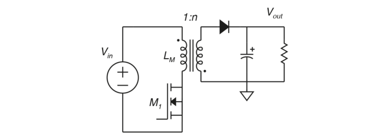
Thanks to its versatility, performance and simplicity, the so-called ‘flyback’ topology – which generally comprises a primary-side MOSFET, output (secondary) rectifier diode, output capacitor and flyback transformer and a few other minor components – has been a popular choice for low-power AC/DC conversion for many years.
Figure 1. Simple flyback converter
A version of the topology known as quasi-resonant (QR) flyback has become particularly popular as it enhances efficiency and performance by reducing switching losses through the lowering of primary MOSFET drain-source voltage before the turn-on pulse. This voltage lowering is achieved using a resonance between the transformer inductance and the parasitic capacitance of the power MOSFET, which reduces the energy dissipated as the parasitic MOSFET capacitance is discharged before the MOSFET is turned on.
Figure 2. Quasi-resonant (QR) flyback converter
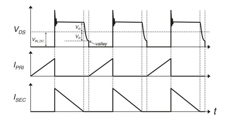
Waveforms of the MOSFET voltage and corresponding primary and secondary currents are shown below.
After the energy stored in the transformer is fully discharged to the secondary, oscillation occurs across the MOSFET drain. This is caused by the primary inductance and the capacitance seen across the MOSFET drain-to-source. The voltage ringing, which depends on the reflected voltage VR, will produce minimum valley points. When the controller detects the minimum valley point, it turns on the MOSFET for QR or valley switching flyback operation.
QR efficiency gains are primarily realized in full-load with 110V AC grid input, when this architecture is at almost Zero Voltage Switching. At light loads, and when the input is 240 V (i.e. EU grid), efficiency is generally lower because hard switching cannot be avoided.
The QR flyback design can be further improved by implementing zero-voltage switching (ZVS). As stated, in a normal QR flyback design the MOSFET is switched in a ‘valley’ where the drain-source voltage (VDS) is at a minimum, but not necessarily zero. With ZVS (or soft switching), VDS falls to zero before the MOSFET is switched. This not only minimizes losses but reduces electromagnetic interference (EMI).
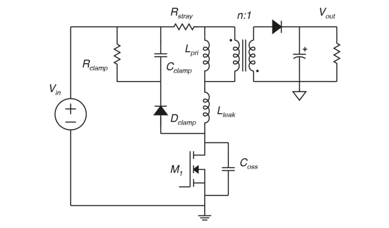
A more recent evolution is active clamp flyback (ACF) architecture, which uses the energy stored in the transformer’s leakage inductance that would have been dissipated in a passive clamp snubber resistor. Delivering this ‘recycled’ energy to the load improves converter efficiency and significantly reduces the peak voltage across the MOSFET during turn-off. What’s more, the QR ‘valleys’ in an ACF design are significantly lower, often achieving near-ZVS operation, supporting reduced switching losses and lower EMI.
Figure 3. Active clamp flyback (ACF) converter
Flyback Evolution
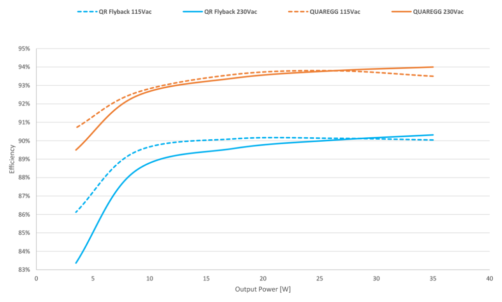
Designers looking to further enhance performance, efficiency and reliability of AC/DC converter designs now have a further option. Known as QuarEgg®, this innovative evolution of the flyback topology significantly improves the efficiency and reduces the size of AC/DC converters that would normally have been based upon ACF and QR flyback topologies. Unlike other approaches, QuarEgg operates with ZVS under all load conditions to give very flat efficiency curves, delivering up to 95% at full load and up to 92% at light load. What’s more, in standby mode, a QuarEgg-based design consumes less than 18 mW.
Figure 4. Comparison of QuarEgg and QR flyback efficiencies
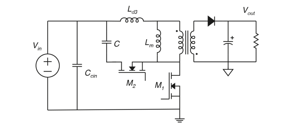
Compared to a generic QR flyback topology, the new approach adds a low-voltage, low-cost MOSFET on the secondary side in parallel to the SR MOSFETs, which is used mainly for the Zero Voltage Switching (ZVS). The main QuarEgg controller is on the secondary side of the converter so as to enhance output voltage regulation, which integrates the synchronous rectification control as well as the power delivery (PD) control. The elimination of a high-voltage, high-side clamping MOSFET reduces overall component count and improves reliability.
Figure 5. Simplified schematic of QuarEgg AC/DC converter
The ZVS MOSFET is essentially included as a means of actively forcing ZVS for the primary power MOSFET across all load conditions. While the converter is switching, the secondary side controller senses the VDS of the primary MOSFET via the secondary winding. When each crest occurs, the ZVS MOSFET turns on, allowing a small amount of current to be injected in the power transformer, after which it turns off and that energy is rectified and recovered at primary side, discharging the drain node so VDS becomes zero, thereby ensuring a ZVS turn-on of the primary MOSFET.
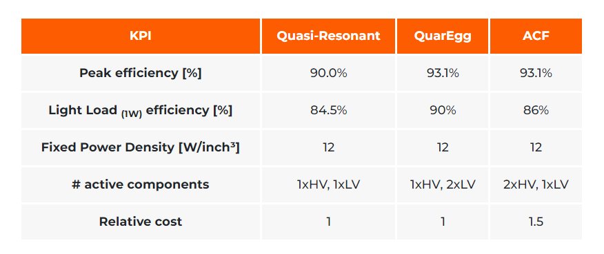
Figure 5. Key KPIs for QR, ACF and QuarEgg AC/DC conversion solutions
The new topology can be used with all types of MOSFET switching devices, including legacy silicon and wide bandgap (WBG) materials such as gallium nitride (GaN) and silicon carbide (SiC). With improved performance compared to conventional ACF and QR topologies, QuarEgg-based power converters are up to seven times more efficient and three times smaller than traditional silicon converters and up to three times more efficient and twice as small as already high-performance GaN converters.
For more information about topology QuarEgg and controller EPIC1AFQ01, we invite you to visit Eggtronic official website at the following links:
Disclaimer: This article has been published with explicit permission from Eggtronic, who has granted Excelpoint the rights to produce and share this content on our platform. All information, insights, and viewpoints are provided in collaboration with Eggtronic, ensuring authenticity and accuracy. No part of this article may be reproduced or utilized in any form or by any means without prior written consent from Eggtronic and Excelpoint.